
 |
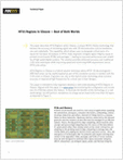
Once you identify critical 3D regions of a PCB (e.g., a staggered via structure) for treatment with the HFSS solver, your results are then seamlessly combined with SIwave’s powerful analysis for fast, efficient and accurate extraction of the entire PCB. This automated solution reduces simulation time and RAM by limiting the scope of the 3D HFSS analysis to the most critical areas, while delivering superior accuracy for high-speed signal nets. You get the gold-standard accuracy of HFSS and the speed of SIwave — the best of both worlds. To demonstrate this one-of-its-kind capability, we used HFSS Regions within SIwave to simulate a server mother board (60 cm by 42 cm) with over 40 layers. At 20 GHz, it’s an electrically large problem of 4000 square wavelengths. Want to know the results? Download the white paper. |