

Three-dimensional integrated circuit (3DIC) design is a semiconductor architecture that stacks multiple chip layers vertically within a single package, connecting them through microscopic channels called through-silicon vias (TSVs) and hybrid bonding. Unlike traditional flat, two-dimensional chip layouts, 3DIC technology places compute logic, memory, and interconnect layers on top of one another, enabling faster data transfer, lower power consumption, and a dramatically smaller physical footprint. As the demands of artificial intelligence workloads have exploded, 3DIC has emerged as one of the most critical frontiers in chip design, and Taiwan-based Alchip Technologies is positioning itself at the center of this shift.
In this article, we’ll discuss how Alchip’s advanced 3DIC platform is changing the way AI and high-performance computing (HPC) processors are designed. We’ll break down why AI chip development is moving from transistor-level improvements toward full system-level integration, explore the specific technologies Alchip is using to solve some of the industry’s hardest engineering problems, and look at what this means for the future of data centers, AI accelerators, and the broader semiconductor market.
TL;DR Snapshot
Alchip Technologies recently announced that its 3DIC platform is driving more efficient development of next-generation AI and high-performance computing chips. The platform uses a hybrid architecture and integrates with Taiwan Semiconductor Manufacturing Company’s advanced packaging technologies.
Key takeaways include…
- Alchip’s 3DIC platform combines horizontal chiplet scaling with vertical die stacking in a hybrid 3.5D architecture, integrated with multiple TSMC advanced packaging technologies including CoWoS and SoIC.
- The platform delivers measurable performance gains, including up to 3-5x higher interconnect density, 30-40% less energy per bit, and up to 35% lower latency compared to conventional approaches.
- AI chip design is shifting from a transistor-level focus to a system-level focus, and Alchip’s unified design flow across silicon, packaging, and system layers helps designers manage that complexity.
Who should read this: Semiconductor professionals, AI hardware engineers, data center architects, tech investors, and AI enthusiasts.
Why AI Chip Design Is Moving to the System Level
For decades, the semiconductor industry has relied on shrinking transistors to improve chip performance. Each new process node brought faster, more power-efficient chips almost automatically. But that playbook is running into hard physical and economic limits. According to a Semiconductor Engineering analysis, the 3DIC market is entering a decisive phase as traditional Moore’s Law scaling delivers diminishing returns in performance per watt, and system architects are shifting toward vertical integration and chiplet-based partitioning to keep making progress.
The problem isn’t just physics. Large monolithic dies, the kind you’d need for a powerful AI accelerator, face what’s known as the reticle limit, which is a hard cap on how big a single chip can be. Larger dies also mean lower manufacturing yields and sharply rising mask costs. Meanwhile, AI workloads are demanding multi-terabyte-per-second memory bandwidth, and data movement is consuming a growing share of total system power.
This is why the industry conversation has shifted from “how small can we make the transistor?” to “how well can we make multiple chips work together as a single system?” It’s a fundamentally different design challenge that requires rethinking how compute dies, memory stacks, and interconnect fabrics are co-designed, packaged, and thermally managed.
What Alchip’s 3DIC Platform Actually Does
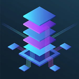
Alchip’s platform tackles this system-level challenge with what the company calls a hybrid 3.5D architecture. Rather than choosing between horizontal chiplet scaling (placing multiple small chips side by side on an interposer) or vertical die stacking (layering chips on top of each other), Alchip’s approach combines both.
According to an April 2026 announcement, the platform integrates with several of TSMC’s advanced packaging technologies, including CoWoS-S, CoWoS-R, CoWoS-L, and TSMC-SoIC-X. The result is high-bandwidth, low-latency die-to-die connectivity that supports multi-terabyte-per-second aggregate throughput.
But the platform isn’t just about stacking silicon, it co-designs die placement, heat dissipation, and power delivery in a unified flow. Shorter vertical power paths and optimized power delivery networks improve efficiency. Integrated thermal strategies are designed to support the advanced cooling approaches that modern data centers require, which is critical when systems are reaching multi-kilowatt power levels.
Johnny Shen, Chairman, CEO and President of Alchip Technologies, framed it this way: the platform gives customers flexibility to architect around their specific workloads while Alchip manages the complexity of integration, packaging, and production. A typical configuration might include multiple compute chiplets on advanced process nodes, I/O dies on more mature nodes, and HBM memory stacks, all within a single package.
The company has also been building toward this moment through a series of technical milestones. In September 2025, Alchip completed the tape-out of a 3DIC test chip that incorporated a 3nm top die and a 5nm base die using TSMC’s SoIC-X packaging technology. And in March 2026, they announced significant progress on 2nm customer device commercialization, including multiple designs in tape-out and customer engagements on full-product 2nm ASIC development.
The Bigger Picture: A Market in Rapid Expansion
Alchip’s platform isn’t emerging in a vacuum, the entire advanced packaging market is surging. A Bloomberg Intelligence report projected that the advanced semiconductor packaging market could reach $80 billion by 2033, with AI driving much of that growth. The report noted that TSMC is expected to maintain over 40% market share in advanced packaging, thanks to its integrated model combining chip fabrication with packaging.
The demand is already straining supply chains. A recent CNBC report noted that Nvidia has reserved the majority of TSMC’s leading CoWoS packaging capacity, and that ASE, the world’s largest outsourced semiconductor assembly and test company, sees advanced packaging sales doubling in 2026.
For companies like Alchip, this creates both opportunity and urgency. As hyperscale cloud providers, AI accelerator startups, and HPC system companies race to build custom silicon, they need design partners that can navigate the full stack of complexity, from the silicon itself to the packaging, thermal management, and production at scale. That’s precisely the gap Alchip’s 3DIC platform is built to fill.
What This Means for the Future of AI Hardware
The shift toward system-level chip design has implications that reach well beyond Alchip’s specific platform, it signals a broader change in how the semiconductor industry thinks about performance. Rather than relying on a single foundry’s process node improvements, chip designers are increasingly treating the entire package as their canvas, mixing and matching dies from different process nodes, stacking memory closer to compute, and using advanced interconnects to tie it all together.
This trend is particularly important for AI. Training large language models and running inference at scale require enormous memory bandwidth and extremely tight coordination between compute and memory. Traditional architectures, where data has to travel long distances between separate chips on a circuit board, create bottlenecks. 3DIC approaches put memory and compute in intimate physical proximity, slashing latency and power consumption for data movement.
The practical implication for organizations building AI infrastructure is that chip design choices are becoming system architecture choices. Picking an AI accelerator isn’t just about clock speeds or transistor counts anymore, it’s about how the entire package has been designed to move data, manage heat, and deliver power. Platforms like Alchip’s 3DIC offering represent the kind of integrated thinking that’s likely to define the next generation of AI hardware.
Frequently Asked Questions
Alchip Technologies is a semiconductor company founded in 2003 and headquartered in Taipei, Taiwan. It specializes in providing ASIC (application-specific integrated circuit) design and production services for companies developing complex, high-volume chips. The company serves customers in AI, high-performance computing, networking, and consumer electronics.
3DIC stands for three-dimensional integrated circuit. It’s a chip design approach where multiple layers of integrated circuits are stacked vertically within a single package, connected by through-silicon vias (TSVs) and hybrid bonding. This vertical stacking enables faster data transfer between components, lower power consumption, and a smaller physical footprint compared to traditional two-dimensional chip designs.
CoWoS, which stands for Chip-on-Wafer-on-Substrate, is an advanced packaging technology developed by TSMC (Taiwan Semiconductor Manufacturing Company). It places multiple chips side by side on a silicon interposer and then mounts that interposer onto a substrate. CoWoS enables high-bandwidth connections between chips, and it’s a key technology behind many of today’s most powerful AI accelerators, including Nvidia’s data center GPUs.
An ASIC, or application-specific integrated circuit, is a chip designed for a particular use case rather than for general-purpose computing. Unlike GPUs or CPUs that can handle a wide range of tasks, ASICs are optimized for specific workloads, making them more efficient for those tasks. In the AI space, companies often develop custom ASICs to accelerate machine learning training or inference at lower power and cost than off-the-shelf chips.
A chiplet is a small, modular piece of silicon designed to be combined with other chiplets inside a single chip package. Instead of building one massive monolithic die, chip designers can create several smaller chiplets, each optimized for a different function (compute, memory, I/O), and connect them using advanced packaging. This approach improves manufacturing yields, reduces costs, and allows designers to mix and match process nodes for different parts of the system.
High-performance computing refers to the use of powerful processors and systems to solve complex computational problems at very high speeds. HPC systems are used in scientific research, weather forecasting, financial modeling, and increasingly, AI model training. Modern HPC systems often rely on advanced chip architectures, including 3DIC designs, to achieve the memory bandwidth and processing power these workloads demand.
Other Enterprise AI Articles You May Be Interested In
OpenAI’s GPT-Rosalind: A New AI Model Purpose-Built for Life Sciences Research
Claude Opus 4.7: Everything You Need to Know About Anthropic’s Latest AI Model
What Is Composable AI Decisioning? GrowthLoop’s New Platform Explained
Adobe’s Firefly AI Assistant: A New Era of Agentic Creativity
Open Source Quantum AI Is Here: Everything You Need to Know About NVIDIA Ising